The most common task when preparing a prototype PCB is generating isolation routing, this is, cutting around the traces for electrical isolation. A not so common task is somehow cutting inside shapes, just following lines. Such task could be useful for engraving the silkscreen (text and lines) into the copper.
Starting with version 7, FlatCAM supports tracing Gerber layers. Let’s dive straight into an example:
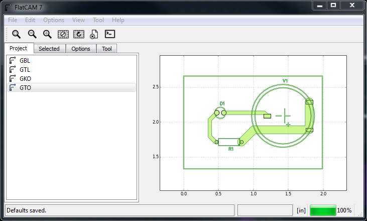
The image below shows an example PCB generated from an online program easyeda.com. Layers shown are bottom (GBL) and top (GTL) copper, board cutout (GKO), and silkscreen (GTO).
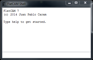
The objective here is to trace the silkscreen. We want to finally obtain g-code that will cut inside/along the lines. We will do this using the FlatCAM Shell. You can open it through the menu Tool→Command Line:
We need to open the desired layer specifying that we want to trace (or follow) the path in the Gerber file, and not to create polygons from it. This has to be done at the time the file is parsed, so we need to open a different copy. Let’s look at the open_gerber command:
> help open_gerber
Opens a Gerber file.
   > open_gerber <filename> [-follow <0|1>] [-outname <o>]
      filename: Path to file to open.
      follow: If 1, does not create polygons, just follows the gerber path.
      outname: Name of the created gerber object.
To enable following/tracing we must set the follow option to 1. Here’s how we open the file:
> cd: C:/path/to/files
> open_gerber GTO -follow 1 -outname GTO_follow
Nothing new should appear on the screen because no polygons were created but the new object GTO_follow should be in the Project list.
Now let’s create some geometry we can see and use to create a CNC Job. This is done with the follow command:
> follow GTO_follow -outname silk_geo
Another object with name silk_geo should be in the list. If we hide all objects except GKO (green) and silk_geo (red) we should see the following:
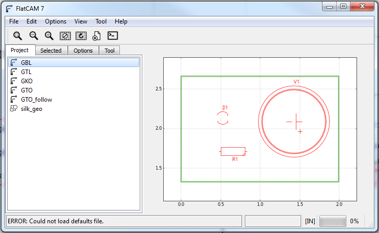
Compare this to the first window shown in this article. Notice that the inner large circle resulted in two red circles. This is because that circle in the Gerber was not defined as a path but probably as a polygon.
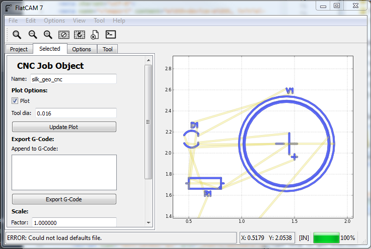
The final step is to create a CNC Job from this new geometry and export G-Code. You can do this in the GUI by double-clicking the silk_geo object, entering the desired parameters and clicking Generate in the Create CNC Job section. This will create an object named silk_geo_cnc and is shown in the screenshot below.
 We can do this in the shell too. To create the CNC Job:
> cncjob silk_geo
To finally create the g-code in the file silk.gcode:
> write_gcode silk_geo_cnc silk.gcode
Of course these commands have additional parameters you can control. You can look them up in the manual or by typing help in the shell.
You can use the g-code you’ve just generate to cut into the copper to label your parts, add a custom logo or perform arbitrary cuts onto your board. But don’t limit yourself to engraving! You can use a permanent marker to write on your boards too or even use a laser source for this purpose.